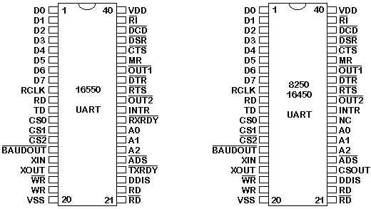
| Pin
No. |
Name |
Notes |
| Pin
1:8 |
D0:D7 |
Data Bus |
| Pin 9 |
RCLK |
Receiver Clock
Input. Its frequency should equal the receiver's baud rate x 16 |
| Pin 10 |
RD |
Receive Data |
| Pin 11 |
TD |
Transmit Data |
| Pin 12 |
CS0 |
Chip Select 0 -
Active High |
| Pin 13 |
CS1 |
Chip Select 1 -
Active High |
| Pin 14 |
nCS2 |
Chip Select 2 -
Active Low |
| Pin 15 |
nBAUDOUT |
Baud Output - Output
from Programmable Baud Rate Generator. Frequency = (Baud Rate x
16) |
| Pin 16 |
XIN |
External Crystal
Input - Used for Baud Rate Generator Oscillator |
| Pin 17 |
XOUT |
Crystal Output (external) |
| Pin 18 |
nWR |
Inverted Write Line |
| Pin 19 |
WR |
Write Line-Not
Inverted |
| Pin 20 |
VSS |
Connected to Common
Ground |
| Pin 21 |
RD |
Inverted Read Line |
| Pin 22 |
nRD |
Read Line - Not
Inverted |
| Pin 23 |
DDIS |
Driver Disable. It
goes low when CPU is reading from UART. Can be connected to Bus
Transceiver if data bus has high capacity . |
| Pin 24 |
nTXRDY |
Transmit Ready |
| Pin 25 |
nADS |
Address Strobe. Used
if signals are unstable during read or write cycle |
| Pin 26 |
A2 |
Address Bit 2 |
| Pin 27 |
A1 |
Address Bit 1 |
| Pin 28 |
A0 |
Address Bit 0 |
| Pin 29 |
nRXRDY |
Receive Ready |
| Pin 30 |
INTR |
Interrupt Output |
| Pin 31 |
nOUT2 |
User Output 2 |
| Pin 32 |
nRTS |
Request to Send |
| Pin 33 |
nDTR |
Data Terminal Ready |
| Pin 34 |
nOUT1 |
User Output 1 |
| Pin 35 |
MR |
Master Reset |
| Pin 36 |
nCTS |
Clear To Send |
| Pin 37 |
nDSR |
Data Set Ready |
| Pin 38 |
nDCD |
Data Carrier Detect |
| Pin 39 |
nRI |
Ring Indicator |
| Pin 40 |
VDD |
+ 5 Volts |